

Instrumentation for electrical transport measurements available in-house is used synergically with electronic nanodevice design and fabrication tools, material properties modeling tools as well as advanced computational resources available within the UNIMORE Scientific Campus.
For device fabrication and material characterization, we use the facilities available at CNR-NANO S3 Modena and CIGS – Interdepartmental Large scale facilities (Centro Interdipartimentale Grandi Strumenti).
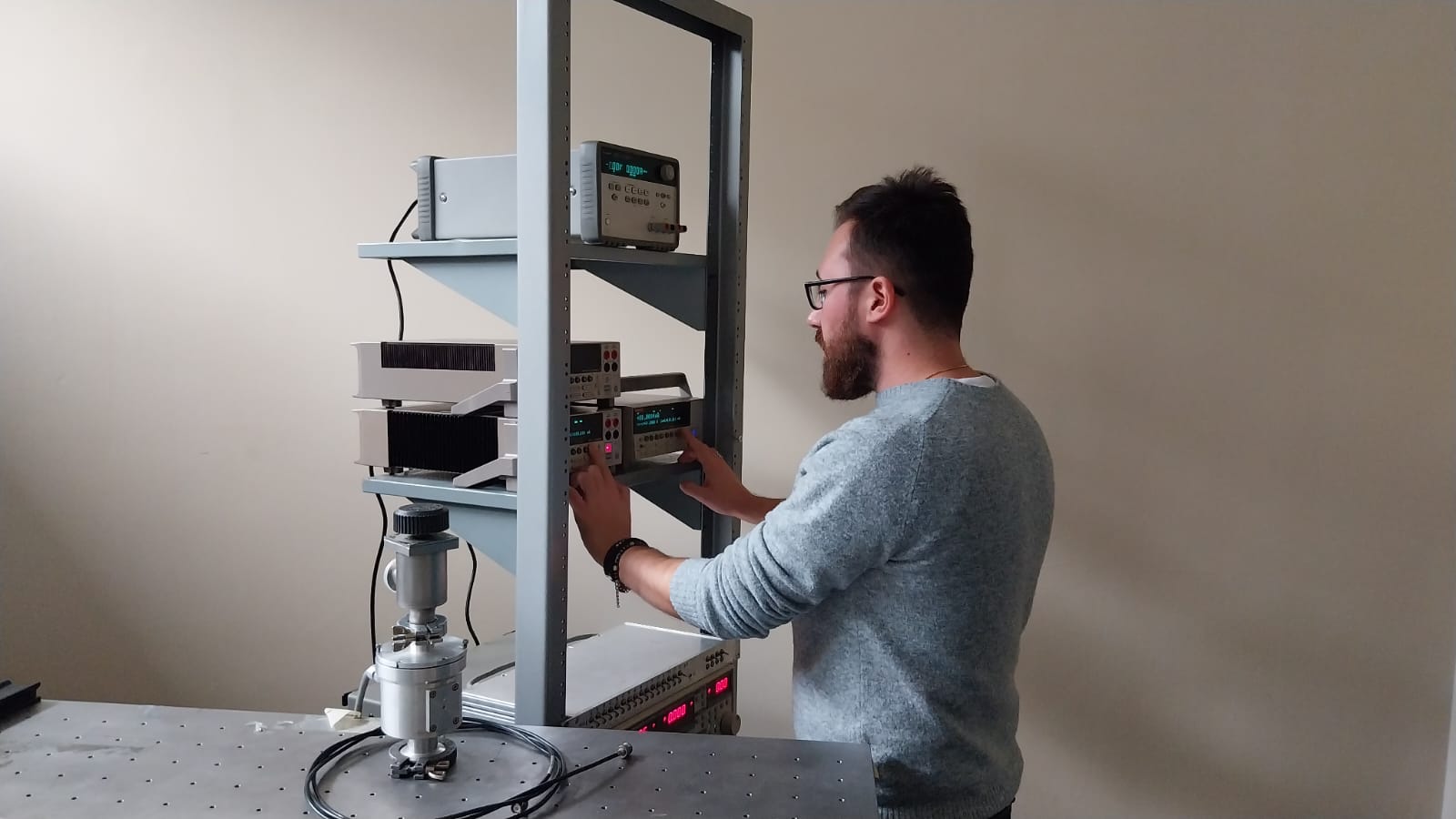
For nanodevice transport experiments, we use measurement setups available in our lab. Engineered devices are measured in different transport regimes and several configurations, ranging from atmospheric pressure and temperature to high vacuum and cryogenic temperatures.
EXPERIMENTAL RESOURCES
Nanomaterial & device imaging and morphological characterization:
In order to characterize the nanomaterials employed for device fabrication, we resort on several instrumentation facilities which include:
- Scanning Electron Microscopy
- Dual beam FIB/SEM
- micro-Raman spectroscopy
- Atomic Force Microscopy

Device fabrication and packaging:
We have more than 10 years’ experience in the use of facilities for nanodevice fabrication and packaging. Our work benefits from the collaboration with Dr. Gian Carlo Gazzadi and Dr. Claudia Menozzi and resorts on the use of :
- UV lithography
- Electron Beam Lithography
- Focused Ion Beam Lithography
- Metal evaporation
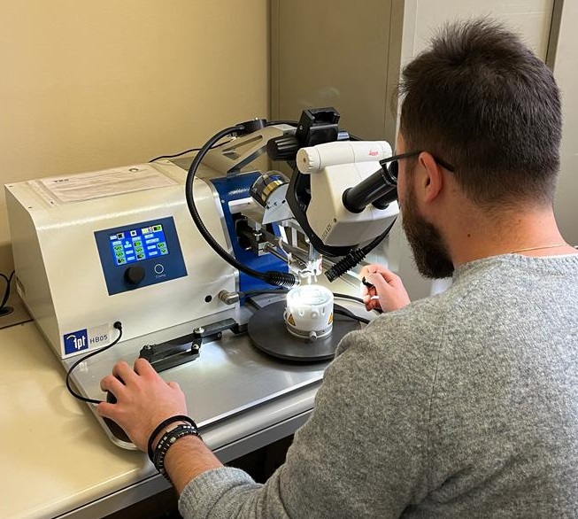
- TPT HB-05 wedge/ball bonder
Classical and quantum transport measurements:
Our transport laboratory is furnished with different measurement setups for each specific application we address:
- 3-Probe optical probe station (300 K, 1ATM, in air)
- Room temperature vacuum chamber (300 K, 10-6 mbar)
- Dry cryostat (base temperature <3 K)
COMPUTATIONAL AND MODELING RESOURCES
DEVICE DESIGN AND MODELING
- Finite Element Modeling (Comsol Multiphysics, Lumerical)
- Electronic design automation software for Integrated circuit layout editing (Elphy Quantum, klayout)
COMPUTATIONAL RESOURCES
- Multicore workstations
- Access to HPC facilities
- Access to D-Wave for quantum systems simulations