

SEMICONDUCTOR-BASED and HYBRID QUANTUM TECHNOLOGIES
After decades in the laboratory, quantum effects are now being harnessed in the real world, and innovative platforms for applications of quantum technologies are explored both in academia and industry.
At the nanoFab we are contributing to the next quantum revolution by investigating quantum phenomena at the nanoscale in semiconductor quantum dots and low dimensional systems and by developing hybrid quantum nanodevice platforms.
Our focus is on nanowire-based devices addressed by QUANTUM TRANSPORT measurements and on IONTRONICS with quantum nanomaterials, as well a on 2D material-based QUANTUM PHOTONIC INTEGRATED PLATFORMS.
“Spin-resolved magneto-tunneling and giant anisotropic g-factor in InAs-GaAsSb core-shell nanowires”. V. Clericò, et al., Nano Letters, 2024, https://doi.org/10.1021/acs.nanolett.3c02559
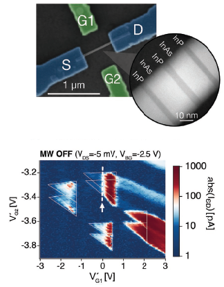
“Calibration-Free and High-Sensitivity Microwave Detectors Based on InAs/InP Nanowire Double Quantum Dots“, Cornia, S., et al., Advanced Functional Materials 2023, 33, 2212517, https://doi.org/10.1002/adfm.202212517
“Polarization Control in Integrated Graphene-Silicon Quantum Photonics Waveguides“. S. Cammarata et al., Materials 2022, 15(24), 8739; https://doi.org/10.3390/ma15248739
“Orbital Tuning of Tunnel Coupling in InAs/InP Nanowire Quantum Dots“, Sadre Momtaz, Z., et al., (2020) Nano Letters, 20, 1693-1699, https://doi.org/10.1021/acs.nanolett.9b04850
ENERGY HARVESTING
The quest towards sustainable energy sources and manipulation is of uttermost importance for our society.
The nanoFab group is developing novel strategies leading to increased efficiency and performance in THERMOELECTRIC DEVICES, HARVESTING ENERGY FROM WASTE HEAT, as well as novel strategies to exploit ULTRAFAST ENERGY TRANSFER mechanisms occurring in nanoscale materials.
“Editorial: focus on waste-heat harvesting via thermoelectric conversion: materials, devices and systems for sustainable energy technologies“. C Artini, et al., 2024 Nanotechnology 35 100201, DOI 10.1088/1361-6528/ad1439
“Structural and Dynamic Characterization of Li–Ionic Liquid Electrolyte Solutions for Application in Li-Ion Batteries: A Molecular Dynamics Approach“, Salvador, M.A., et al., (2023) Batteries, 9, 234, https://doi.org/10.3390/batteries9040234
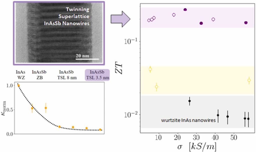
“Giant reduction of thermal conductivity and enhancement of thermoelectric performance in twinning superlattice InAsSb nanowires”. L. Peri et al., Nano Energy 103, 2022, 107700, https://doi.org/10.1016/j.nanoen.2022.107700
“Electrostatic Control of the Thermoelectric Figure of Merit in Ion-Gated Nanotransistors”, D. Prete et al., Adv. Func. Mat., 31: 2170275, 2021. https://doi.org/10.1002/adfm.202170275
IONTRONICS and SENSING
Electrolyte solutions and ionic signals are ubiquitious in nature, especially in biological signal transmission. Furthermore, ions provide ultra-intense local electric fields that can be tailored to control large-aspect-ratio semiconductor nanostructure devices.
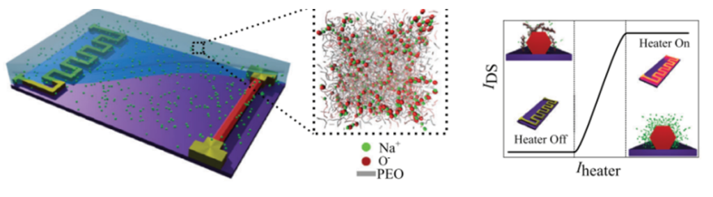
At the nanoFab we are engineering innovative devices combining inorganic nanostructures and organic ionic conductors. These include ion-gated and ion-sensitive field effect transistors that may perform as HIGH-PRECISION TEMPERATURE SENSORS, as sensors for biological analytes as well as bio-electronic transducers.
Furthermore, nanoFab is focusing on the development of innovative nanoscale systems allowing for LOW PERTURBATION DETECTION OF CHARGED-PARTICLE BEAMS with ultra-high spatial resolution, virtually down to individual atoms.
“Heat-Driven Iontronic Nanotransistors”, D. Prete et al., Advanced Science 2023, 2204120, https://doi.org/10.1002/advs.202204120
“Ultrafast Photoacoustic Nanometrology of InAs Nanowires Mechanical Properties“, Gandolfi, M., et al., (2022) Journal of Physical Chemistry C 126, 6361-6372, https://doi.org/10.1021/acs.jpcc.2c01060
“Impact of electrostatic doping on carrier concentration and mobility in InAs nanowires“, Prete, D., et al., (2021) Nanotechnology 32, 145204, https://doi.org/10.1088/1361-6528/abd659
“Conductometric sensing with individual InAs nanowires”, Demontis, V., et al., (2019) Sensors 19, 2994, DOI: 10.3390/s19132994